- 您现在的位置:买卖IC网 > Sheet目录537 > XR18W753IL48-F (Exar Corporation)IC RF TXRX 868-956MHZ 48QFN
�� �
�
�XR18W753�
�REV.� 1.0.0�
�SINGLE� CHIP� 868MHZ� TO� 956MHZ� RF� TRANSCEIVER�
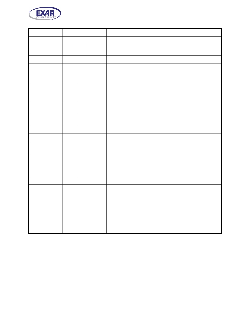
�N� AME�
�TEST2�
�P� IN�
�31�
�T� YPE�
�Digital� I�
�D� ESCRIPTION�
�Factory� Test� Mode.� For� normal� operation,� this� pin� should� be� connected�
�to� GND.�
�A2�
�A3�
�CLK_OUT+�
�CLK_OUT-�
�MODEM_RESET�
�VREG_CLK_EN�
�32�
�33�
�34�
�35�
�36�
�37�
�Digital� I�
�Digital� I�
�Digital� O�
�Digital� O�
�Digital� I�
�Digital� I�
�I2C� Address� bit-2�
�I2C� Address� bit-3.� This� address� line� should� be� connected� to� GND.�
�16� MHz� LVDS� digital� clock� outputs.� Connect� pin� 35� to� ground� for�
�CMOS� clock� output.�
�Digital� modem� reset� (active� high,� level� sensitive).�
�Voltage� Regulator� and� crystal� oscillator� enable� (active� high,� level� sensi-�
�tive)�
�AVDD19�
�XTAL1�
�38�
�39�
�Power� I�
�Analog� I�
�VDD� (1.9V� ±� 0.1V)� for� crystal� oscillator� and� clock� divider.�
�16MHz� crystal� input� or� external� clock� input.� Based� on� typical� PCB� stray�
�capacitance,� a� 27� pF� capacitor� to� GND� is� recommended.�
�XTAL2�
�40�
�Analog� I�
�Crystal� output,� 27� pF� capacitor� to� GND� is� recommended.� If� an� external�
�clock� is� used� at� XTAL1,� this� input� should� be� left� unconnected.�
�AGND�
�DVDD_OUT�
�DVDD�
�41�
�42�
�43�
�Ground�
�Power� O�
�Power� I�
�Ground� for� crystal� oscillator� and� buffers.�
�Decoupling� pin� for� digital� VDD,� 10� nF� capacitor� to� GND� recommended.�
�Digital� Power� Supply,� DVDD� =� 2.2� -� 3.6V.� DVDD� and� AVDD� should� use�
�the� same� power� supply.� 100nF� capacitor� to� GND� recommended.�
�AVDD�
�44�
�Power� I�
�Analog� Power� Supply,� AVDD� =� 2.2� -� 3.6V.� DVDD� and� AVDD� should� use�
�the� same� power� supply.� 100nF� capacitor� to� GND� recommended.�
�AVDD_OUT�
�45�
�Power� O�
�1.9V� stabilized� analog� VDD� output.� This� output� should� be� connected� to�
�all� AVDD19� pins.� 1uF� ceramic� capacitor� to� GND� recommended.�
�AVDD19�
�AVDD19�
�AVDD19�
�PADDLE�
�46�
�47�
�48�
�49�
�Power� I�
�Power� I�
�Power� I�
�Ground�
�Analog� VDD� (1.9V� ±� 0.1V)� for� ADC� and� DAC.�
�Analog� VDD� (1.9V� ±� 0.1V)� for� ADC.�
�Analog� VDD� (1.9V� ±� 0.1V)� for� IF� strip,� TX� mixers� and� both� I/Q� dividers.�
�The� center� pad� on� the� backside� of� the� 48-QFN� package� is� metallic� and�
�is� not� electrically� connected� to� anything� inside� the� device.� It� must� be�
�soldered� on� to� the� PCB� and� may� be� optionally� connected� to� GND� on� the�
�PCB.� The� thermal� pad� size� on� the� PCB� should� be� the� approximate� size�
�of� this� center� pad� and� should� be� solder� mask� defined.� The� solder� mask�
�opening� should� be� at� least� 0.0025"� inwards� from� the� edge� of� the� PCB�
�thermal� pad.�
�Pin� type:� I=Input,� O=Output,� I/O=� Input/output,� OD=Output� Open� Drain.�
�5�
�发布紧急采购,3分钟左右您将得到回复。
相关PDF资料
XS-B14-CB2RB
SENSOR TEMP/HUM/LIGHT BATT XBEE
XT09-4II-RA-NA
MODEM RF 900MHZ RS232/485 NEMA 4
XT09-DK-MESH
KIT DEV 900MHZ W/MESH
XT09-MI
MODULE RF 900MHZ 1W 115K W/MMCX
XT09-PKI-EA-NA
MODEM RF 900MHZ 1W ETHER INT
XT09-SI
MODULE RF 900MHZ 1W 115K W/RPSMA
XU-A11
X-STICK 2.4GHZ USB TO XBEE
XV-8000CB :3 50.3000KHZ+/-60DPS
AUTOMOTIVE GYRO SENSOR +/-60DPS
相关代理商/技术参数
XR18W753L48-0A-EB
功能描述:界面开发工具 900MHz RF EVAL Board
RoHS:否 制造商:Bourns 产品:Evaluation Boards 类型:RS-485 工具用于评估:ADM3485E 接口类型:RS-485 工作电源电压:3.3 V
XR1901SN
制造商:Electro-Term/Hollingsworth 功能描述: 制造商:Electro-Term/Hollingsworth 功能描述:16-14awg No. 6 stud ring terminal - FAC STK
XR1902SN
制造商:HOLLINGSWORTH 功能描述:16-14awg No. 8 stud ring terminal - FAC STK
XR1903SN
制造商:HOLLINGSWORTH 功能描述:16-14awg No. 10 stud ring terminal - FAC STK - 1k in house
XR1906SN
制造商:HOLLINGSWORTH 功能描述:16-14awg 1/4 stud ring terminal - FAC STK
XR1906SNT
制造商:Electro-Term/Hollingsworth 功能描述:
XR1907S
制造商:Electro-Term/Hollingsworth 功能描述:
XR1907SN
制造商:HOLLINGSWORTH 功能描述:16-14awg 5/16 stud ring terminal - FAC STK